全部
▼
搜索
熱搜:
位置:中冶有色 >
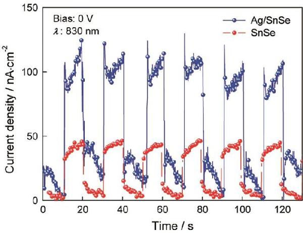
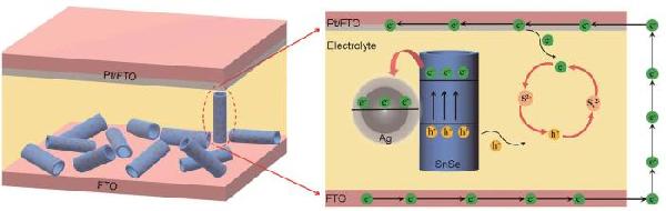
> 自供能Ag/SnSe納米管紅外探測器的制備和性能研究
 924
編輯:中冶有色技術(shù)網(wǎng)
來源:方向明,任帥,容萍,劉爍,高世勇
924
編輯:中冶有色技術(shù)網(wǎng)
來源:方向明,任帥,容萍,劉爍,高世勇

 分享 0
分享 0
 舉報(bào) 0
 收藏 0
收藏 0
 反對 0
反對 0
 點(diǎn)贊 0

 中冶有色技術(shù)平臺
雜有色金屬資源清潔利用學(xué)術(shù)論壇")
 2025年03月21日 ~ 23日
 創(chuàng)新大會(huì)") 2025年03月28日 ~ 30日
2025年03月28日 ~ 30日 術(shù)會(huì)議") 2025年03月28日 ~ 30日
2025年03月28日 ~ 30日 材料焊接與連接技術(shù)交流會(huì)") 2025年03月28日 ~ 30日
2025年03月28日 ~ 30日 資源科技創(chuàng)新發(fā)展論壇") 2025年04月27日 ~ 29日
2025年04月27日 ~ 29日